Standard-cell characterization
Standard-cell characterization refers to the process of compiling data about the behavior of standard-cells. Just knowing the logical function of a cell is not sufficient to build functional electrical circuits. There are more aspects to be considered: For example the speed of a single cell will influence the speed of the full circuit, such as the power used by a single cell can influence the total power. Further, the speed as well as the power might be influenced by the output load. Standard-cell characterization aims at collecting this sort of information. This article focuses about characterization by transistor-level simulations. A comprehensive work on characterization can be found in [1].
Prior to the characterization automated tools can perform a transistor-level analysis of the cell to automatically find the type of the cell. This step is also called 'recognition' or 'functional abstraction' and can be used to guide the characterization flow. Standard-cell recognition is treated in a separate article about Standard-cell recognition.
Background
A standard-cell can be looked at from different abstraction views:
- Logic (Boolean function)
- Schematic (Connection pins only)
- Netlist (Internal circuit made of transistors)
- Netlist with parasitics
- Physical Layout
- Timing (Delays, hold and setup times, ...)
- Power
- Noise
Usually, some of the views are given by design and others must be derived. For instance, the logic function of a NAND gate could be defined as "!(A & B)". In principle all other views can be derived from this equation using some additional assumptions and constraints depending on the technology and design goals. The netlist of combinatorial cells can be generated algorithmically (TBD: reference). Starting from the netlist a layout will be drawn which can be used to extract parasitic capacitances and resistances within the cell. The resulting netlist of transistors and parasitics can further be used to get an abstract description of the cells timing, power and noise behavior.
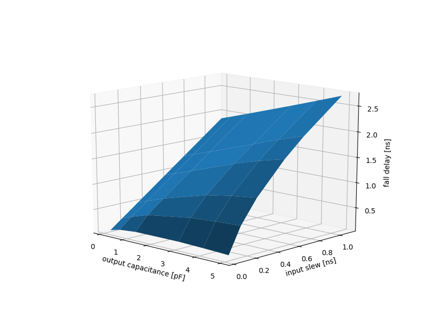
A way to derive timing and power numbers is simulation of the transistor netlist. However, one simulation is not enough because the cells behavior strongly depends on other factors such as PVT (process variations, operating voltage, temperature), input wave form and output load. A common approach is to look at best and worst PVT conditions. Effectively this allows to predict lower and upper bounds on the cell behavior which are important to ensure the overall functionality of the design. Further, cells must be characterized over a reasonably large range of input edge rates and output load. For example, a cell could be characterized on a two dimensional grid with variable input edge rate and output load (non-linear delay model). If the grid points are chosen correctly then the behavior between grid points can be approximated by linear interpolation.
Liberty File Format
The 'liberty' ('.lib') file format is often used to store library information such as logic functions of cells together with their timing behavior. One liberty file will contain information of multiple standard-cells (library). It is common to have multiple liberty files for the same library: One for each PVT corner. The most basic setup could consist of two liberty files: A worst-case file (low voltage, high temperature, worst case delays, ...) and a best-case file (high voltage, low temperature, ...).
Timing
Timing views of standard-cells typically consist of delays (time between a change in input and change in output), edge rate and constraints (setup, hold, recovery, removal).
Trip Points
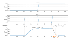
Timing measures require to define events that can be used to measure delays. Usually such an event is defined by the instant a signal crosses a given threshold or trip point. Different trip points can be used for delays and edge rates. It is not uncommon to also use different trip points for rising and falling edges. By appropriately choosing trip points that are further away from 50% one can get extra timing margins.
The following snipped shows the trip point definition in the liberty file of the FreePDK45:
slew_upper_threshold_pct_rise : 80;
slew_lower_threshold_pct_rise : 20;
slew_upper_threshold_pct_fall : 80;
slew_lower_threshold_pct_fall : 20;
input_threshold_pct_rise : 50;
input_threshold_pct_fall : 50;
output_threshold_pct_rise : 50;
output_threshold_pct_fall : 50;
Conditional & Default Timing Arcs
The timing behavior from input to output usually depends not only on the input port but also on the levels of the other inputs. For the characterization process this means that all input combinations must be considered. The liberty file format allows to store timing information conditional on other inputs. However, during circuit synthesis the input signals are not known and synthesizers rely on a default timing arc. The choice of the default timing arc depends on the characterization corner. For combinatorial gates the longest timing arc should be chosen for the worst-case (setup) corner and the shortest arc should be chosen for the best-case (hold) corner. Even if not used by the synthesizer conditional timing arcs might still be useful for post-layout simulation (e.g. verification of clock domain crossing) and power analysis because glitching will be modeled more accurately.
Model types
The point of characterization is to create abstract representations of a physical device's behavior. The general approach is to find a mathematical model that allows to describe the behavior with the required accuracy. For each device the model is fitted to parameters that have been measured in a simulation or in physical experiment. Below is a incomplete list of common model types.
Non-linear model (NLM)
The non-linear model approximates two dimensional scalar functions by evaluating them on a bounded grid (not necessarily equidistant) and by using interpolation to find function values between grid points. Function values outside of the grid bounds are found by extrapolation which may lead to large errors depending on the choice of the grid bounds and grid points.
Choosing grid bounds
Grid points and bounds need to be chosen such as to minimize the approximation error. The grid bounds are therefore given by the parameter ranges that are expected to appear in a design. For a delay model the minimum output capacitance could be chosen by the smallest input capacitance among all cells whereas the maximum output capacitance could be chosen to be the largest capacitance that can be driven with the strongest cell such that the resulting edge slope is still acceptable. The maximum output capacitance may also be defined by electro-migration rules of the PDK. The minimal input slew can be simulated by applying a step-function to the strongest inverter available in the library and measuring its output slew. The maximum input slew will be given by the weakest cell driving the maximal acceptable output load. Note that the grid bounds should be consistent over the library. At least cells of the same drive strength class should share the same grid bounds to avoid erroneous extrapolation when comparing cell delays during synthesis.
Choosing grid points
The following algorithm illustrates how a low number of grid points can be chosen while ensuring an upper bound of the approximation error:
- Evaluate the function on the minimum and maximum bound.
- Evaluate the function half-distance in-between and check if the interpolated value would be accurate enough.
- If it is accurate enough: done. Otherwise: include the new point and recursively repeat the algorithm on the new intervals.
Scalable polynomial model
TBD
Composite current source model (Synopsys CCS)
TBD Similar to the non-linear model but instead of output voltage the output current is measured and stored.
Effective current source model (Cadence ECSM)
TBD
Delays and Edge Rate
Setup and Hold
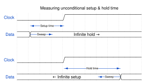
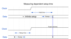
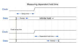
Setup and hold times are constraints and in contrast to delays they cannot be measured by a single distance measurement. To find either setup or hold time multiple simulation runs are necessary whereby the data edge is moved towards the clock edge until failure of the storage element is detected. Instead of moving the signal edges it is much more efficient to do a bisection search in practice.
<figure id="fig:indep_and_dep_setup_hold_time">
</figure>
Failure types of sequential elements
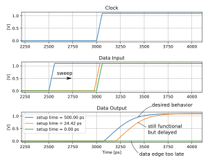
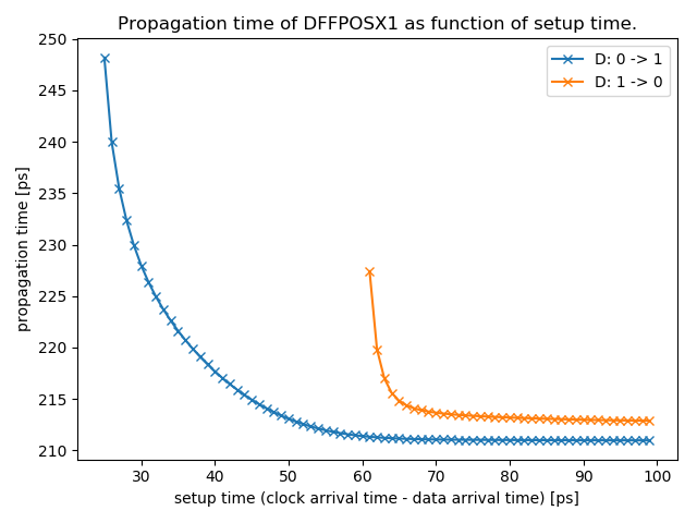
Failure of a storage element regarding setup and hold time is a matter of definition. The most obvious type of failure happens when the input signal is applied in a way that the storage element fails to sample the data. When pushing the data edges closer and closer to the clock edge one can observe that the propagation delay steadily increases before the sampling totally fails. The output signal is pushed out by the approaching input signal. Increase of the propagation delay should also be treated as a failure because it could endanger the constraints of the following longest path.
The minimal (or also nominal) clock-to-output delay can only be achieved with very large setup and hold times. To allow for shorter setup/hold times, a degradation of the clock-to-output delay can be accepted. This is often denoted with the roll-off factor, which defines an acceptable relative increase of the clock-to-output delay in percent. Since the clock-to-output delay can be zero or negative (depending on how it is measured) a relative roll-off factor might not be the best choice. Instead also absolute values are used to specify the maximum allowed push-out time (maximum value by which the clock-to-output delay may be enlarged). Also explained here..
The maximum allowed push-out time must be chosen carefully. If it is close to zero, then large setup and hold times will be chosen which minimizes the clock-to-output delay but decreases the maximum clock-frequency of a circuit. Choosing a large maximum allowed push-out time leads to shorter setup and hold times but may cause actual setup or hold violations or meta-stability issues in a design.
As a starting point it might be interesting to find setup times such that the sum of setup time tsu and resulting clock-to-output delay td is minimized (same for the hold time). This implies that dtd/tsu = -1. This describes the point where the plot of clock-output-delay versus setup time has slope -1.
Independent setup and hold times
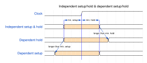
The independent minimal setup time is the minimal setup time that can be achieved when the hold time is infinitely long, i.e. when the input data signal remains stable forever after the clock edge.
Similarly the independent minimal hold time is the minimal hold time that can be achieved when the setup time is infinitely long, i.e. when the input data signal is already stable since an infinite time before the clock edge.
Dependent setup and hold
Setup and hold times cannot be found independently. Measuring minimal setup and hold time independently will result in a too small setup/hold window. Simulations will show that the minimum setup time pushes the hold time away from the clock edge and vice versa as shown in <xr id="fig:indep_and_dep_setup_hold_time" />. This effect can be significant. For this reason setup and hold times should not be measured independently. There are trade-offs to be made: If the setup time is chosen as small as possible, then the dependent hold time will need to be significantly larger than the minimal hold time in order to meet the desired clock-to-output delay. For some applications it might be interesting to know the minimum setup+hold window which likely does not correspond to the independent minimal setup and hold times. In other words there are three interesting minimization objectives (but many possible trade-offs in between):
- minimize setup time, minimize dependent hold time afterwards: Setup time is chosen to be minimal, hold time is chosen dependent on setup time. This could be useful for flip-flops connected to paths with a long delay.
- minimize hold time, minimize dependent setup time afterwards: Hold time is chosen to be minimal, setup time is chosen dependent on hold time. This could be useful for flip-flops connected to paths with a short delay.
- minimize (setup time + hold time): The total setup/hold window is minimized. This could be useful for asynchronous signals because minimizing the setup/hold window also lowers the susceptibility window for meta-stability.
Minimal setup+hold
Minimal setup+hold is the narrowest time window where the data signal must remain stable such that it is properly sampled by the flip-flop, i.e. the clock-to-output delay is bounded by the desired output delay.
Finding minimal setup+hold such that a desired clock-to-output delay is met can be done as follows:
Express the setup and hold times in terms of a time window of a certain width and with a center shifted by some amount relative to the clock edge.
- Start with a guess of the time window. Set window center to 0 (at the same time as the clock edge). The guess must be large enough such that the flip-flop samples the data.
- Shift the center of the window such that the clock-to-output delay is minimized. Update the window center.
- Find the window width such that the resulting delay equals the maximum allowed delay. Update the window width.
- If tolerance is not met: Continue at 2. Otherwise return the result.
The step 2. involves optimization of a scalar function with a single variable. The step 3. involves root-finding of a scalar function in one variable. A method like bisection can be applied.
Power
TBD
Noise
TBD
Software
- LibreCell (librecell-lib)
- Yagle
- CharLib
- libretto
- vsdStdCellCaracterizer
Literature
References
- ↑ Engineering the CMOS Library, Enhancing Digital Design Kits for Competitive Silicon, David Doman, ISBN 978-1-118-24304-6
